Screen Printing Equipment for Precise PCB Solder Paste Application
BUILT FOR ACCURACY
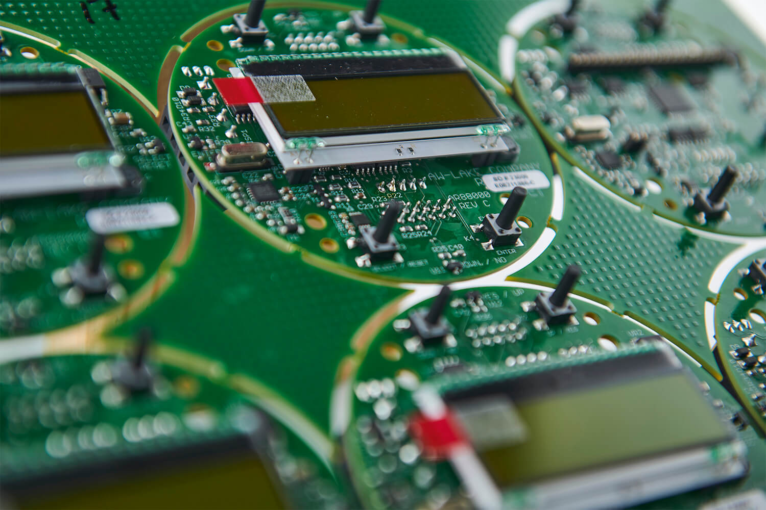
Precision Solder Paste Printing
Repeatable Deposits for Reliable Assemblies
At ETI, screen printing PCB assemblies starts with one principle: precision at this stage determines reliability at every stage that follows. Our screen printing equipment applies solder paste with exceptional accuracy — ensuring optimal component placement, consistent joint formation, and the kind of repeatable results that complex, high-reliability assemblies demand. From first-article prototypes and small-batch NPI runs to steady-state mid-volume production, our process is built to perform without compromise.
WHY IT MATTERS
Why Solder Paste Screen Printing Is the Most Critical Step in SMT
The Foundation for Downstream Quality
Solder paste screen printing is where the SMT process either gets set up for success or quietly introduced to failure. A precisely deposited paste layer — consistent in volume, correctly registered to each pad, and cleanly released from the stencil aperture — is what enables reliable joints, accurate component placement, and clean reflow outcomes. Get it wrong here and the consequences compound: bridging, insufficient solder, and misalignment that no downstream process can fully correct.
ETI’s PCB solder paste printing capabilities use advanced automated screen printers equipped with high-precision vision alignment systems — capable of holding tight tolerances on fine-pitch components and high-density boards.
HOW IT WORKS
Your Printed Circuit Board Assembly Partner

Stencil Preparation
Every job starts with a high-quality, laser-etched stainless steel stencil engineered to your design and manufactured to IPC-7525 guidelines. Fiducial marks give our global positioning system the reference points they need to achieve consistent, repeatable registration from the first board to the last.

Precise Stencil Alignment
Advanced vision systems recognize fiducial marks and automatically align the stencil to the PCB before each print cycle. This automated PCB stencil alignment is what makes fine-pitch work — 0.4mm pitch and smaller — reliably manufacturable at production volumes, eliminating the registration drift that causes offset-related defects.

Solder Paste Application
Squeegee pressure, print speed, and blade angle are precisely controlled and documented for each assembly. The result is uniform paste volume and consistent deposit geometry across every aperture — whether the job calls for leaded or RoHS-compliant paste formulations.

Post-Print Inspection Readiness
Our screen printers employ a vision system that identifies the amount of solder paste applied and rejects the panel based on the criteria we set. Any deposit that doesn’t meet specification is caught before a single component is placed — not after reflow when correction is costly.
This entire process integrates with our DFM review, where our engineering team identifies potential stencil or print challenges before production begins, reducing iterations and protecting your schedule.
PROJECT BENEFITS
Key Benefits for Your Project
Unmatched Accuracy
Our solder paste screen printing process consistently meets IPC-A-610 Class II and III standards — giving you the confidence that boards built for medical devices, aerospace systems, or industrial controls are being assembled to the right level of rigor.
Consistency Across Volumes
ETI is purpose-built for the small-to-mid-volume work that high-capacity contract manufacturers deprioritize. Our NPI process supports validated small-batch builds before full production commitment, helping engineering teams reach the market up to 30% faster without sacrificing process integrity.
Reduced Risk on Complex Assemblies
Precise PCB solder paste printing is especially consequential on boards destined for harsh-environment applications — medical devices, aerospace avionics, heavy equipment controls — where a field failure is never just a rework event. Our upstream controls exist specifically to prevent downstream risk.
Vertical Integration Advantage
Screen printing at ETI isn’t a standalone step handed off to a separate team. It feeds directly into our in-house component placement, reflow, selective soldering, AOI inspection, X-ray, and conformal coating — all managed under one roof by a single accountable team. There’s no handoff ambiguity, no subcontractor gap, and no disconnect between what was printed and what was built.
Proactive Quality, Documented and Certified
Our ISO 9001:2015 certification and IPC-certified training program mean our process controls aren’t aspirational — they’re documented, audited, and continuously improved. Every print run parameter is logged and traceable.
WHY ETI
Why Engineering and Procurement Teams Choose ETI
Most contract manufacturers treat solder paste application as a routine setup step. ETI treats it as the foundation the entire assembly is built on. That difference in philosophy shows up in yields, in first-pass inspection results, and in the conversations our team has with yours when something needs to be optimized.
Our mid-market focus also means you get something that disappears at larger CM shops: direct access to experienced people, fast quote turnaround, and a team that already knows your project when you call. Whether you’re a design engineer validating a new medical device or a procurement manager qualifying a new assembly partner for agricultural equipment controls, you’ll deal with specialists — not a ticket queue.

Ready to Discuss Your PCB Assembly Requirements?
Talk to a specialist about how ETI’s screen printing capabilities can support your next project. Upload your files for a fast, no-obligation quote.