Selective Soldering and Wave Soldering for Complex PCB Assemblies
PROCESS EXPERTISE
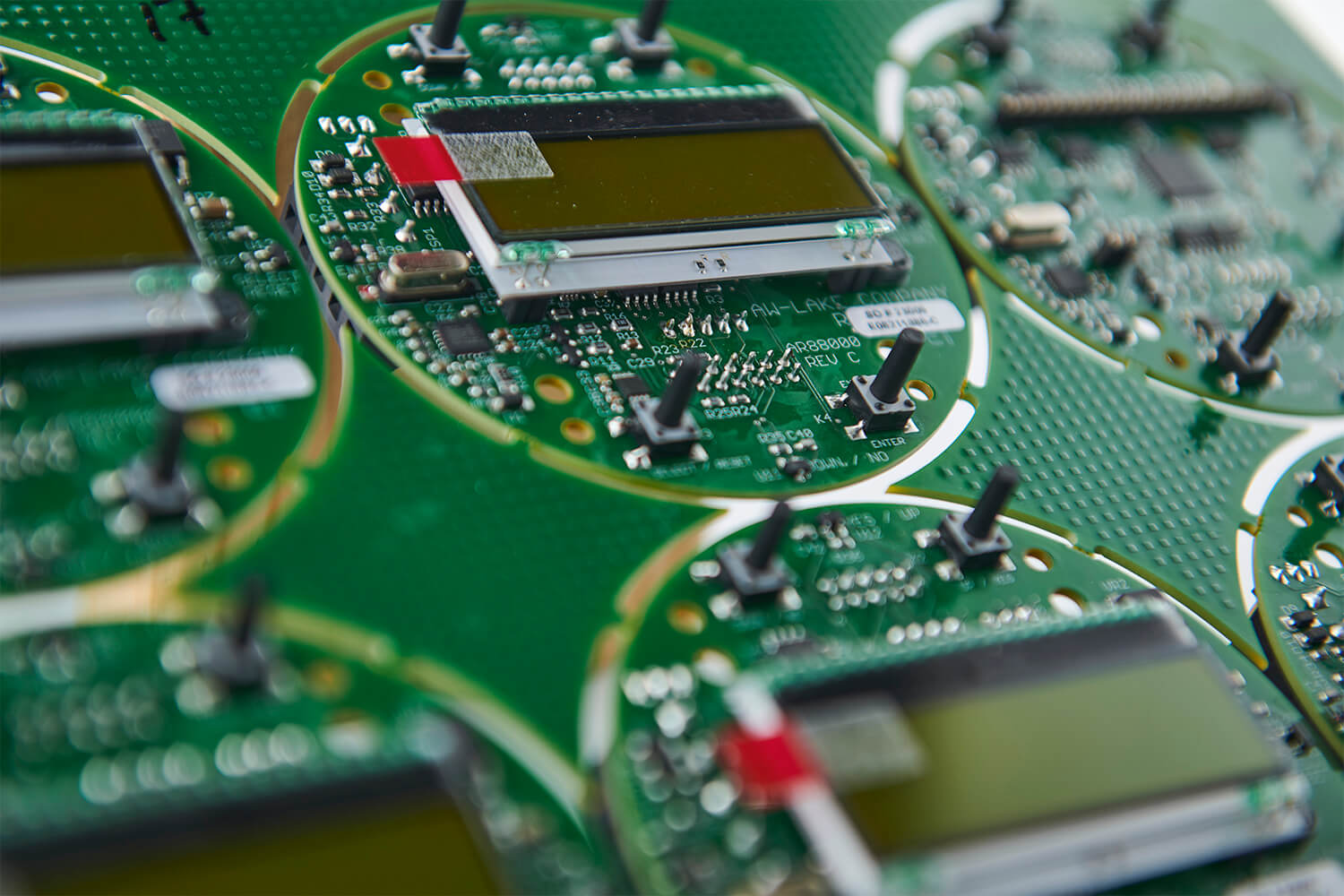
PCB Soldering Methods for Complex Assemblies
Choosing the Right Process for Your Board
At ETI, reliable PCB assembly soldering isn’t a single process. It’s a decision made thoughtfully based on your board design, component mix, and application requirements. Our facility runs both selective soldering equipment and wave soldering capabilities, giving our engineering team the flexibility to match the right process to your specific assembly and the expertise to know the difference.
KEY DIFFERENCES
Wave Soldering vs. Selective Soldering: Understanding the Difference
When Each Method Makes Sense
For procurement managers and engineering teams evaluating PCB soldering methods, the choice between wave and selective soldering isn’t arbitrary. It’s driven by board architecture, component density, and the thermal constraints of your design. Understanding when each process is appropriate is where a knowledgeable contract manufacturing partner earns its value.
Wave Soldering
Wave soldering passes the underside of a populated PCB across a continuous wave of molten solder. It’s a high-throughput process well-suited for through-hole dominant boards or assemblies with bottom-side SMT components that have been adhesive-bonded prior to soldering. The entire bottom surface of the board contacts the solder wave simultaneously, making it efficient for boards with predictable, uniform layouts and no thermally sensitive components that could be damaged by full-board solder exposure.
Selective Soldering
Selective soldering takes a more surgical approach. A selective soldering machine with a point-to-point nozzle system and infrared heaters delivers solder only to specific through-hole joints on an otherwise populated board, soldering individual locations without exposing adjacent SMT components, connectors, or thermally sensitive areas to the solder wave.
The machine lets us adjust the nozzle size to precisely match the pad and lead geometry, producing a higher-quality solder joint and avoiding excess solder that can create defects. For connectors with multiple leads, we can also use drag soldering. The nozzle travels along the row of leads on one side, then the other, which is significantly more efficient than repeated point-to-point cycles.
This makes selective soldering the process of choice for complex mixed-technology assemblies where through-hole components co-exist with dense SMT populations on both sides of the board assembly that can’t tolerate broad thermal exposure.
For the hybrid assemblies that make up the majority of ETI’s work, boards that blend SMT and through-hole components across a single design, selective soldering is often the right answer. It’s more precise, more protective of the broader assembly, and better suited to the complex, high-reliability boards our customers bring to us.
HOW IT WORKS
How ETI’s Soldering Process Works
Controlled Soldering from Start to Finish
Pre-Soldering Preparation
Before any board reaches the solder equipment, our team reviews component placement, through-hole geometry, and thermal requirements as part of our DFM process. Masking or tooling fixtures are prepared where needed to protect areas of the board that shouldn’t see flux or solder. This upfront investment in preparation is what prevents defects, not just detects them.
Flux Application
Controlled flux application precedes soldering in both processes. For selective soldering, a spray fluxer applies flux only to the joints that will be soldered, and the process runs under nitrogen to maintain an inert atmosphere. Flux chemistry, volume, and application method are selected based on your solder paste specification, board finish, and compliance requirements.
Solder Application
Wave soldering: Boards travel through a precisely controlled solder pot at a defined speed and angle.
Selective soldering: The machine targets individual joints with programmable nozzle positioning, dwell time, solder flow, and infrared heaters that ensure consistent heat to both the board and components.
ETI runs multiple solder alloys depending on customer specifications and the intended application of the board assembly. Our wave soldering line uses two dedicated pots, one lead-free (RoHS) and one leaded, and we support military and aeronautics programs that still require leaded solder. The pot is mounted on a trolley, allowing us to cool it down and swap pots as needed so we can run the right alloy for each job.
Post-Solder Inspection
Every soldered assembly moves to inspection, visually by IPC-certified operators and, where warranted, through our 3D AOI and in-house X-ray capabilities. Through-hole joints and hidden connections that can’t be evaluated visually are candidates for X-ray analysis, ensuring joint integrity before the board moves forward.
WHY IT MATTERS
Selective Soldering on Complex Mixed-Technology Boards
Protecting Quality on Dense, Hybrid Designs
The trend in PCB design toward higher component density and mixed-technology assemblies has made selective soldering increasingly important. When your board carries a dense SMT population alongside through-hole connectors, power components, or legacy parts that can’t be converted to surface mount, selective soldering is often the only process that can deliver consistent, defect-free joints without damaging what’s already been placed and reflowed.
Real-World Example
On one assembly, wave soldering applied too much heat too often and caused connectors to warp. Switching to selective soldering solved the problem immediately. Less heat, applied less often, eliminated the warpage while maintaining excellent joint quality.
For the industries ETI serves, medical devices, aerospace electronics, HVAC controls, industrial equipment, and agricultural machinery, this isn’t a theoretical advantage. These are boards that go into demanding operating environments where a cold joint, a solder bridge, or a thermally stressed component creates real consequences.
PRODUCT BENEFITS
Key Benefits of ETI’s Soldering Capabilities
Flexibility, Precision, and Process Control
Process Flexibility
Running both wave and selective soldering under one roof means the process recommendation you get from ETI is based on what’s right for your board, not what equipment happens to be available.
Precision on Complex Assemblies
Selective soldering gives our team joint-level control on boards where board-level thermal exposure would create risk.
Small Batch Capability Without Process Compromise
Whether we’re running 25 boards or 2,500, the same fixturing, flux controls, and individually developed temperature profiles apply. Your NPI validation build is process-representative of your production run.
Single-Source Integration
Soldering at ETI sits in the middle of fully integrated PCB lines. Boards with through-hole joints arrive from reflow with a known-good SMT population, go through selective or wave soldering, and move directly to AOI and X-ray inspection, all within the same facility, managed by the same team.
Compliance and Certification
Our soldering processes support both leaded and RoHS-compliant assemblies and are executed under ISO 9001:2015 certified process controls by IPC-certified operators.
WHY ETI
Why ETI for PCB Assembly Soldering
Engineering-Led Decisions, Not Line-Level Guesswork
At high-volume contract manufacturers, soldering process decisions often get made by whoever is running the line that day. At ETI, they are made by manufacturing engineers who understand your design, your application environment, and your quality requirements, and who have the equipment to execute the right process, not just the available one.
Our mid-market focus means you’re working with a team that has capacity for your volumes, attention for your complexity, and accountability for your outcomes.

Ready to Talk Through Your Soldering Requirements?
Whether you’re evaluating wave soldering vs. selective soldering for a new design, troubleshooting yield issues on a current assembly, or qualifying a new contract manufacturing partner, ETI’s team is ready to get into the details with you.